
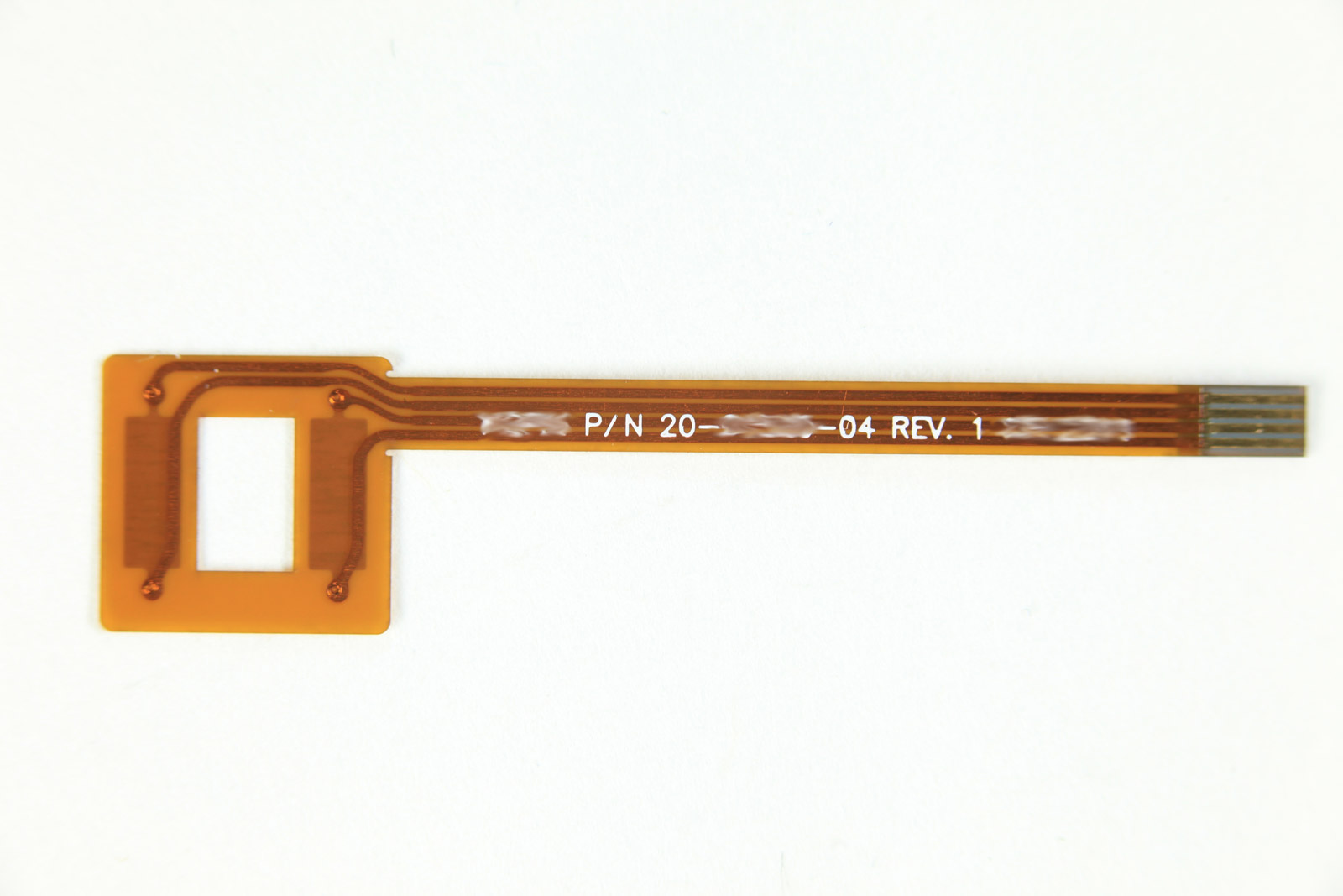
Micro Via and Flex Circuit Panels
Micro Vias
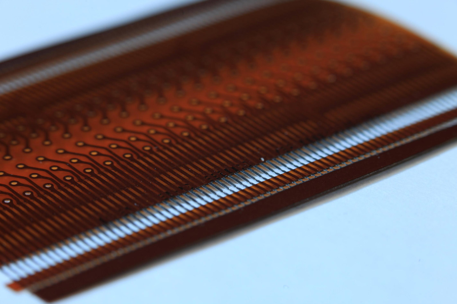
Microvias are holes through one or more layers of a flexible circuit board made of alternating insulating and conducting layers of material. These materials are often copper sheet (1/2 oz typically) and an epoxy/fiberglass blend in thin sheets (.001-.002” thick). The laser drilling tool will create a via from the top layer down to a copper catch pad below which will be plated to form an electrical connection between conducting layers.
The drilling, and subsequent plating works best when the diameter of the via is equal to or greater than the depth of the via (a 1:1 ratio is ideal). Accu-Tech regularly generates vias in the range of .003” to .008” (.075-.100mm) with capability to produce smaller and larger sizes.
Our systems can align to pre-etched openings in the top layer and remove the dielectric down to the next layer. Supplying pre-etched openings in the top layer may be more cost effective – depending on your etching capabilities. Pre-etched boards can have a quicker turn around time.
Registration targeting is usually a set of four “butterfly” targets, one at each corner of the panel just outside of the pattern of the part or parts. The supplied computer files will show the relationship of the targets to the via pattern and allow our systems to compensate for slight shrinkage and out of square conditions that can be an outcome of the lamination process.
Guidelines for Via Drill Files and prepping panels:
1) We can accept .DRL files (ideal), Gerber or .DXF files.
2) Files must have different via sizes called out as different tool numbers all in the same file. One file per side/layer.
3) Fiducials should be identified as a separate tool number as well. We prefer these targets to be under .020” and can be of the butterfly type, or similarly bulls-eye, circular pad or cross-hair type.
4) It is helpful to include tooling holes or landmarks to help quickly identify panel orientation.
5) Please send a panel stack-up showing the thickness of materials we are drilling through and landing on. This will help us in reducing the time for test patterns which reduces cost to you.
6) Ideally, any overhanging copper flashing from lamination can be pre-trimmed from the boards before delivery as this excess material can prevent the boards from laying flat on the laser tooling as well as reduce consistency of features.
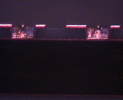
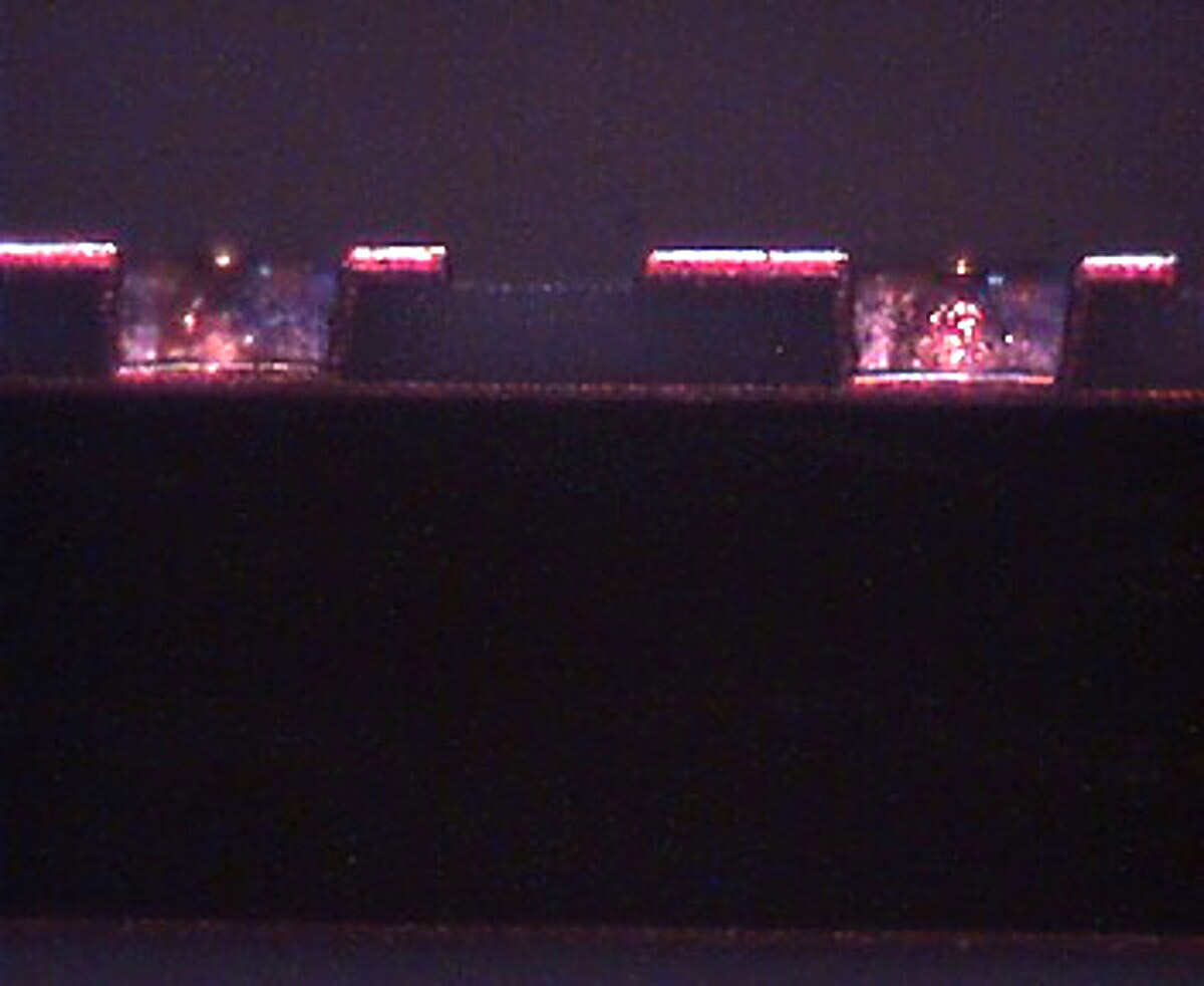
Circuit Singulation/Separation – Flex Circuits
 The laser is an excellent tool for precision separation of circuits generated in an array on flex panels. The laser’s very small ‘tool size’ and no contact forces may be beneficial to either small part size or parts with chip components already attached.
Our lasers generate very little smoke or deposits on the edges of the parts, as a result, reducing cleaning time on your end. Our fixtures prevent parts from dropping or displacing after the final cut reducing risk to fragile parts. For additional cost, we can accommodate flexible circuits with stiffeners and/or components applied.