
Tech Notes
Micro Via and Flex Circuit Panels TECH NOTE
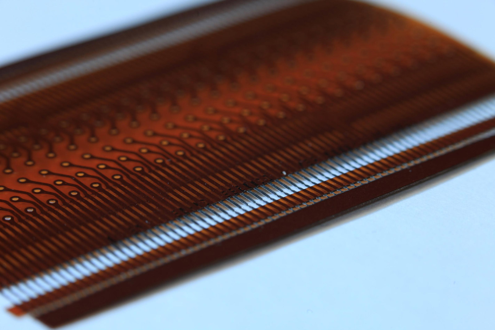
Micro Vias – Generally described as a via or hole through one or more layers of a flexible circuit board made of laminations of alternating insulating and conducting layers of material. These materials are often copper sheet (1/2 oz typically) and an epoxy/fiberglass blend in thin sheets (.001-.002” thick). The laser drilling tool will create a via from the top layer down to a copper catch pad below which will be plated to form an electrical connection between conducting layers.
The drilling, and subsequent plating works best when the diameter of the via is equal to or greater than the depth of the via (a 1:1 ratio is ideal). Accu-Tech Laser regularly generates vias in the range of .003” to .008” (.075-.100mm) with capability to produce smaller and larger sizes.
Our systems can align to pre-etched openings in the top layer and remove the dielectric down to the next layer, or create openings in a solid copper top layer aligned to your lower layer registration fiducials and then remove the dielectric. Supplying pre-etched openings in the top layer may be more cost effective – depending on your etching capabilities. Pre-etched boards can have a quicker turn around time than boards that require laser to make an opening in the top copper.
Registration targeting is usually a set of four “butterfly” targets, one at each corner of the panel just outside of the pattern of the part or parts. The supplied computer files (usually gerber or .drl format) will show the relationship of the targets to the via pattern and allow our systems to compensate for the slight shrinkage and out of square conditions that can be an outcome of the lamination process.
Ideally, any overhanging copper flashing from lamination will be pre-trimmed from the boards before delivery as this excess material can prevent the boards from laying flat on the laser tooling and reduce consistency of features across a panel.
Guidelines for Via Drill Files:
1) We can accept .DRL files (ideal), Gerber or .DXF files.
2) Files must have different via sizes called out as different tool numbers all in the same file. One file per side/layer.
3) Fiducials should be identified as a separate tool number as well. We prefer these targets to be under .020” and can be of the butterfly, bulls-eye, circular pad or cross-hair type.
4) It is helpful to include tooling holes or landmarks to help quickly identify panel orientation.
5) Please send a panel stack-up showing the thickness of materials we are drilling through and landing on. This will help us in reducing the time for test patterns which reduces cost to you.
We at Accu Tech Laser Processing can help you achieve your product designs with our decades of laser experience.
Circuit Singulation/Separation – Flex Circuits
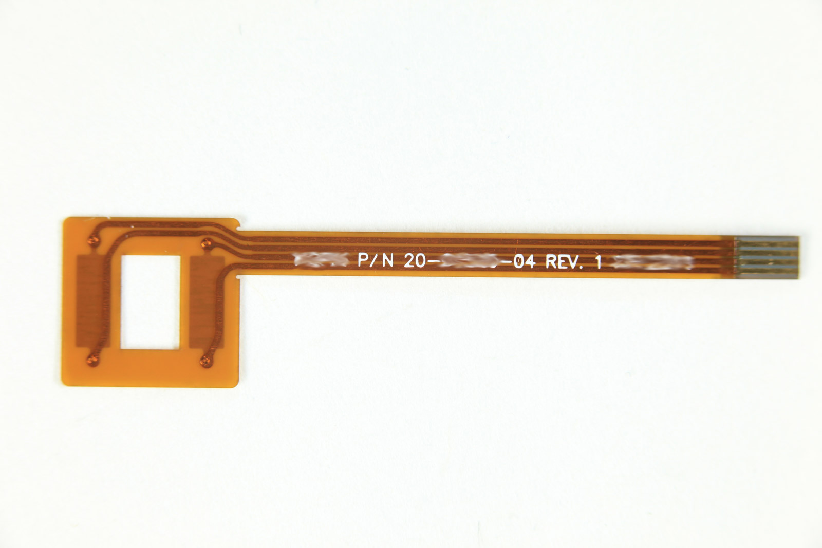
The laser is an excellent tool for precision separation of circuits generated in an array on flex panels. The lasers very small ‘tool size’ and no contact forces may be very beneficial to either small part size or parts with chip components already attached.
Our lasers generate very little smoke or carbon deposits on the edges of the parts which reduces cleaning time on your end. Our fixturing prevents parts from dropping or displacing after the final cut reducing risk to fragile parts. For additional cost, we can accommodate flexible circuits with stiffeners and/or components applied. In most cases, we can hold flex circuit accuracy to +/- .001” or better.
Ceramic TECH NOTE
-Laser Drilling and Machining of Ceramic Substrates
APPLICABILITY
This document provides general guidelines and considerations for the laser drilling and machining of fired ceramic substrates typically used in the manufacture of microelectronic circuits and multichip modules. The specifications and tolerances given here will generally produce the MOST COST EFFECTIVE design approach. Tighter tolerances may be achieved at some increased cost and leadtime.
PURPOSE OF LASER DRILLING AND MACHINING
The CO2 laser has become an important tool in the precision fabrication of technical ceramics. The reasons for this are in the technological changes that have occurred within the electronic industry to miniaturize parts and produce them using batch fabrication methods.
A brief history:
-In the early days of ceramic substrate fabrication, individual substrates where small in overall size, relatively thick, and substrate features were generally large. These small parts were typically metalized one-at-a-time using automated feeders and loaders. The state of the art in substrate tolerances was +/- 1%.
-Early fabrication methods in fired ceramic involved machining substrate features with carbide, diamond or ultrasonic tools. Although these techniques were not really cost effective and were limited in the type and size of features they could create, there were all that was available at the time when precision locations of features were required.
-A subsequent method was developed that utilized precision tooling to punch the required features in “green” ceramics before firing. This method improved the cost situation when the quantities produced justified the cost of prototyping and tooling. Tolerances improved but were limited by variations in the firing process. Green punching technology can be quite effective for volume production runs where substrate features are relatively large and the lot-to-lot and part-to-part tolerances are +/- 1% or larger. Feature size is generally limited to holes or shapes greater than 0.010 in. across the smallest dimension.
-In recent years the high circuit densities and cost reduction efforts demanded by the electronic industry have required that batch fabrication methods be used to cost effectively manufacture ever shrinking miniature substrates. As a result, new hardware, tooling, and techniques have been developed to fabricate multiple parts with high precision on large substrate sheets.
-Under these pressures, the CO2 laser has developed into the most precise and versatile method of fabricating ceramic substrates. Under software control the laser can create features of virtually any planar shape and can maintain tolerances to within +/-0.001 in. The laser is extremely flexible and permits close location of features with considerable layout flexibility. Hard tooling is not required, turnaround is quick, and the cost is low.
-The combination of green punching and laser machining can be cost effective for manufacturing substrates with large, non-critical holes and small, high density features requiring precision.
TYPES OF CERAMIC MATERIALS
Materials covered include thin, flat substrates of Alumina, Aluminum Nitride. Call the Accu-Tech facility directly for technical information on other special materials that may be laser machined.
GENERAL MATERIAL CHARACTERISTICS
Alumina, 96%
Excellent overall substrate material for cost effective manufacturing and laser processing. Typically represents over 90% of the microelectronics volume.
Alumina, 99+%
Similar to 96%. Provides a superior surface for fabricating Thin Film circuitry.
Aluminum Nitride
Roughly equivalent in heat conductivity to Beryllium oxide but the safety issue is avoided. Call Accu-Tech for additional information on Aluminum Nitride.
SUBSTRATE SIZE AND LIMITS
Typical Substrate Size: 4.5” X 4.5” – Larger sizes can be processed.
Typical Substrate Thickness: 0.010 in. TO 0.060 in. – Thickness greater than 0.100 can be processed.
COST EFFECTIVE DRILLING OF HOLES
In order to achieve cost effective manufacturing, multiple parts are typically created on a single large substrate. The parts are then processed in batch form and later singulated into individual substrates by breaking along scribe lines. The processing of either individual substrates or arrays requires accurate registration at each operation.
SUBSTRATE ALIGNMENT OPTIONS
Several options for alignment of laser produced features to the substrate edges are listed below in order of increasing laser processing cost.
1. SCRIBED OUTSIDE EDGES – After scribing the substrate, the borders are broken off to produce accurate outside reference edges for the subsequent processing operations.
2. AS-FIRED OUTSIDE EDGES – The pattern to be cut by the laser is located on the substrate in relation to the original edges. Two adjacent edges on the substrate are used to form a reference corner. The entire substrate can be utilized with this method but the alignment accuracy may be poor due to irregularities in the fired edges.
3. ALIGNMENT FLATS – The alignment repeatability can be improved for subsequent processing by the addition of precision, laser machined flats along the outside reference edges of the substrate. These flats provide a smooth surface to make accurate contact with the tooling pins. Using this method avoids the expense of laser machining the entire substrate edge.
4. POST ALIGNMENT – With this method, cut features can be optically aligned to the substrate metalization or other surface features such as holes, edges or other existing scribe lines. Accuracy is excellent.
Figure 1 illustrates a substrate designed with breakaway borders into which three alignment flats have been machined. The substrate is shown being registered against three alignment pins. For illustration purposes there are sixteen individual parts (defined by scribe lines) shown on the substrate. Each part contains six holes and a cutout that requires laser machining.
FIG. 1 – Substrate Registration using Alignment Flats
METHODS OF LASER DRILLING HOLES
There are two basic methods of creating a hole:
1. Pulsed or percussion method
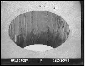
This method is suitable for drilling small round holes up to 0.005 in. by rapidly vaporizing the substrate material at high laser power. Hole creation is very fast and clean. The illustration in Figure 2 shows the cross-section of a drilled hole. The hole shape is dependent on energy distribution within each laser pulse.
Fig. 2 – Cross section – Laser Cut Hole
2. Contoured or trepanned method
This method is used to produce a hole of any size or shape. The method consists of selecting a punch- through point inside the periphery of the feature, cutting to the feature edge, and then following the edge outline to complete the cut that defines the feature.
Fig. 3 – Photo of Laser Contoured Hole
THE ANATOMY OF A LASER CUT
The method of hole creations (either pulse or contour) does not materially affect the cross-sectional shape of the cut edge. The sketch in Figure 2 shows the cross-section of a typical laser cut edge. The laser beam has entered at the top and exited at the bottom. As the beam vaporizes the material, the entrance edge becomes slightly rounded. The cut also develops a slight taper. See the table on at end of this document for the taper vs thickness.
DESIGNING MACHINED FEATURES
Virtually any planar shape can be cut in ceramic substrates. These shapes include circles, curves, rectangles, polygons, rounded objects, thin slots, etc., and any combination of the above. Since ceramics are strong but brittle materials, the designer should consider a radius as large as practical on inside corners. All inside corners will have a minimum 0.002 in. radius due to the laser beam diameter. Rounding outside corners can also reduce chipping.
An important consideration when designing a machined feature is the location of the start and stop points for the cut.
Some general guidelines:
-Provide for the location of the start and stop points in a benign area away from corners. For example when cutting a rectangle, a start point near the center of an edge is ideal.
-Provide clearance around the area where the laser will punch through so that a potential slag bump or chip will not affect the adjacent features.
LAYOUT CONSIDERATIONS
In order to ensure a high yield of finished parts, the designer should attempt to maintain at least the minimum recommended distance between the edges of features, generally greater than the thickness of the substrate.
-Avoid aligning scribe lines and machined features in such a way that the break along the scribe line might deviate to include the machined feature.
-When parts in an array are separated by waste strips, the recommended width of the waste strip should be 0.10” or greater.
DEALING WITH SURFACE MATERIALS
Other materials may appear on the surface of a ceramic substrate or within the substrate and affect the cutting of the substrate.
Examples include:
-Metalization- Such as thick film or deposited thin film metals.
-Metalization on the surface tends to reflect the laser energy. The result can be a slight change in the kerf line and an undercutting of the ceramic beneath the metalization. Cutting through metal on the laser entrance side can cause discoloration of the cut edge.
-Metalization on the backside in contact with the laser beam tends to melt and bead.
-Refractory metalization within the substrate can protrude slightly from the cut edge.
-Dielectrics-Such as glasses or polymers.
Glass dielectrics may tend to chip when cut, especially on the exit side of the laser beam.
Polymers may be affected when the laser beam approaches within 0.002 to 0.005 in.
-Components such as chip capacitors, chip resistors, and semiconductors may cause clearance problems or require special fixturing.
The effect of these materials may be minimized with proper layout and good laser machining techniques.
HANDLING AND CLEANING
Substrates are generally coated with a water soluble material to protect them during scribing, breaking, machining or shipping. The coating may be removed by water wash. Normally, the coating is removed by Accu-Tech unless otherwise specified by the customer.
REMOVAL OF SLAG
Slag occurs when the substrate material is melted by the laser. Slag buildup is primarily found on the beam exit side of the substrate and is removed after laser processing.
TOLERANCES FOR DRILLING AND MACHINING
For best correlation of hole diameter, pin gauges are recommended.
As a general rule it is helpful to coordinate and/or specify specific measuring methods when attempting to measure dimensions and tolerances of the magnitude shown here.
Feature location tolerance………… +/-.002, centerline to centerline.
Kerf width……………………………… .003 +/-.001 measured at the beam exit side.
Slag………………………………………. .001, Max. residual after removal
-Laser Scribing of Ceramic Substrates
APPLICABILITY
This document provides the General Guidelines and Considerations for the laser scribing of ceramic substrates that are typically used in the manufacture of Microelectronic Circuits and Multichip Modules. The specifications and tolerances given will generally produce the MOST COST EFFECTIVE design approach. Tighter tolerances may be achieved at increased cost and leadtime.
PURPOSE OF SCRIBING/SCORING
Scribing makes possible the cost effective manufacture of arrays (multiple ceramic parts) that may be then singulated by breaking them apart. Scribing also provides a cost effective means of improving part quality by allowing the removal of the outside borders that contain defects such as rough or non-parallel edges.
TYPES OF MATERIALS SCRIBED
Typical materials scribed are thin, flat substrates of Alumina, and Aluminum Nitride. Please call the Accu-Tech factory directly for technical information on other special materials that may be scribed.
GENERAL MATERIAL CHARACTERISTICS
Alumina 96%
-Most commonly used in Microelectronics.
-Represents over 90% of the volume manufactured.
-Excellent overall substrate material for cost effective manufacturing and laser processing.
Alumina 99+ %
-Similar to 96% but typically provides a superior surface finish for fabricating Thin Film circuitry.
Aluminum Nitride
-Roughly equivalent in heat conductivity to BeO but the safety issue is avoided. Call Accu-Tech for additional information on this material.
DIMENSIONAL CONSIDERATIONS
Typical Substrate Size: 4.5 in. X 4.5 in. – larger sizes can be processed.
Typical Substrate Thickness: 0.010 in. to 0.060 in. (thickness to .100 in. can be processed.
The processing of arrays involves the registration of the substrate at each operation. Precise alignment at each step is of critical importance. Alignment is typically accomplished by registering the part against three pins where two are located along one edge of the part and one on an orthogonal edge. Since “as fired” or scribed edges may lack the required precision, an additional step to laser machine alignment flats may be required. The figure below (fig. 1) shows substrate alignment flats registered against the alignment pins.
SCRIBE CHARACTERISTICS
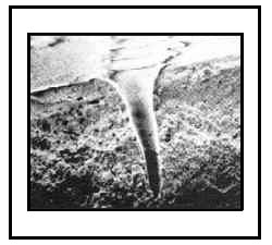
A laser scribe line consists of a series of small, closely spaced holes in the substrate that are produced by pulses of laser energy. Viewed under magnification, the scribe holes should appear essentially clean and free of recast. Under backlighting a plugged hole will appear dark. An occasional plugged hole will not affect the scribe. Hole depth is controllable and should generally be 1/3 to 1/2 of the substrate thickness.
SEM PHOTO OF SCRIBE PULSE HOLE
The SEM photo above shows a cross-section of the tapered hole that has been created by the penetration of a laser pulse into the substrate. The minor amount of slag shown on the substrate surface has been deposited around the hole as a result of the melt. The slag is benign, and is usually removed by a scraping process if the substrate has not been metallized.
The hole depth can be measured by inking the scribe line with a black marker pen, snapping the substrate at the scribe line, and viewing the cross section with a calibrated microscope.
LAYOUT /LOCATION OF SCRIBE LINES
The distance from a scribe center line to the edge of other features such as holes, cutouts, or metalization should be 0.010 to 0.050 inch minimum, depending upon the part design.
The border width or distance from the last scribe line to the edge of the substrate should be 0.100 inch, minimum. The border areas are shown in the figure below. Alignment flats have been laser machined into the borders to permit precision alignment of the substrate into work fixtures.
It is recommended that the scribe lines should completely cross the border areas to produce a good break and clean, square corners when the parts are singulated.
New graphic for this
THE FINISHED PART
In the drawing above, the finished part is shown as being separated from the array. A corner of this part is magnified to show the somewhat rough edges that normally result when singulating a part from a scribed substrate. In applications where the edge roughness must be overcome, the scribe lines can be laser machined at an increased cost.
SUBSTRATE COATING
Substrates are generally coated with a water soluble material to protect them during scribing, breaking, machining or shipping. The coating may be removed by water wash. Normally, the coating is removed by Accu-Tech unless otherwise specified by the customer.
SCRIBING AND ALIGNMENT OPTIONS
AS-FIRED EDGES – The laser scribe pattern is located on the substrate in relation to the original edges. Two adjacent edges on the substrate are used to form a reference corner. The entire substrate can be utilized with this method but the alignment accuracy irregularities in the original edges.
SCRIBED EDGES – After scribing the substrate, the borders are broken off to produce accurate outside reference edges for subsequent operations.
ALIGNMENT FLATS – Alignment repeatability can be improved by the addition of precision, laser machined flats along the outside reference edges of the substrate. These flats provide a smooth, accurate surface to make contact with tooling pins. The expense of having to laser machine the entire substrate edge is avoided.
POST SCRIBING – Using this method, the scribe lines can be optically aligned to substrate metallization or other surface features such as holes, edges or other existing scribes.
SINGULATION OF THE SUBSTRATES
Even with the best scribing, the ability to hold extremely tight tolerances after the break will depend on the substrate material and the skill of the operator. Skilled hand breaking is usually preferred to machine breaking.
Common effects of breaking that cause a variation from a “perfect” straight line are hooks or flares, breakouts, and chips. The majority of these defects occur at the ends of the scribe line and the corners where scribe lines cross each other. The examples below show common variations encountered when breaking substrates. The specifications section below provides cost effective guidelines for acceptance.
INSPECTION OF SCRIBED SUBSTRATES
The following equipment or its equivalent is recommended for the inspection of scribed/snapped substrates.
Ceramic thickness – Micrometer
Substrate Features, distances, locations – Optical Coordinate measurement machine
Pulse spacing, Scribe Depth, Hole Taper, Pulse Hole Diameter, HAZ, Slag Height –
Microscope with calibrated graticule
Breakout Tolerances – Calipers
Camber – Parallel Plates
TOLERANCES FOR SCRIBING
NOTE (1) Pulse spacing tolerance is +/- 0.001 in.
Surface Slag height, Max. .001″
Scribe Location Tolerances
NOTE: All measurements made to a scribe line are made to the scribe centerline.
Scribe, line to line +/-.001″ before snap/break
Scribe, line to laser machined feature +/-.002″
Lasered feature to scribed exterior edge for ceramic thicknesses of
.010 to .030 +/-.003″
.035 to .060 +/-.005″
Scribe line with respect to a fired edge +/-.005
Duroid TECH NOTE
Tech Notes
-Precision Laser Cutting of PTFE Substrates for High Frequency Circuits
APPLICABILITY
This document provides general guidelines and considerations for laser cutting PTFE laminates used in the manufacture of high frequency and microwave circuits. Precision PTFE laminates are used as substrates in the construction of amplifiers, filters, mixers, couplers, phase shifters, transmitters, antennas, etc. PTFE laminate sheet material is sold under the Duroid, Ultralam, Cuclad, Diclad and other trade names.
TYPES OF LAMINATE MATERIALS
The laminates typically used in microstrip, stripline and multilayer circuit fabrication consist of PTFE (Polytetraflouroethylene) that has been reinforced with either glass fibers, woven glass fabric, or proprietary ceramic materials. Certain types of filler materials are used to control the substrate dielectric constant and its temperature coefficient.
PHYSICAL AND MECHANICAL CHARACTERISTICS
Laminates are normally supplied with copper or brass cladding that may be etched and then die cut or precisely machined into the final circuit configuration. The completed laminates are typically between 0.005 and 0.060 inches thick and are clad with 0.125 to 0.5 oz. per ft2 copper. The laminates may then be assembled into an electronic module that serves as a ground plane, a mounting base, and a heat sink. In other cases, the laminates may be bonded to a thick metal plate that serves as the mounting base and the heat sink.
CUTTING LAMINATES REQUIRES PRECISION
Considerable dimensional precision and stability are required of the fabricated circuits to obtain acceptable performance at high frequency. This is particularly true for microstrip and stripline circuits. It is not uncommon to require that line width and spacing dimensions be held to within ± 0.001 inch and that dimensional stability over temperature be less than 25 PPM per C. Workmanship during fabrication must be absolutely meticulous to avoid scratches and micro-dents to edges and surfaces.
The non-rigid nature of unbonded laminates together with the required dimensional tolerances place a substantial demand on the quality and creativity of fixtures, tooling, and workmanship.
CIRCUIT LAYOUTS ARE CHALLENGING
Layout patterns for high frequency circuits are often complex. Additional complexity is created by layout nesting techniques that are employed to fully utilize costly laminate materials. Finally, the fabrication drawings provided may be somewhat inadequate to ensure a precision fit in a housing. Dimensional “fine tuning” may be required to optimize performance of the circuit.
CIRCUIT FABRICATION METHODS USED
Fabrication methods currently used in the industry consist of six basic manufacturing processes:
Masking and etching
Routing with a router
Cutting with a CO2 Laser
Through-hole plating
Drilling with a bit
Punching with a die set
COMPARISON OF CIRCUIT FABRICATION METHODS
Precision photo masking and etching are generally adequate to produce metal patterns of the desired accuracy on the substrate. The table below attempts to qualitatively show three common methods used to shape a laminate substrate. The “best” method will depend on the laminate materials, the geometry of the specific circuit configuration, the tooling available, and, as in most precision operations, the skills, tools, and ingenuity of the operator. The selection of a skilled, experienced, and committed supplier is the best recommendation for achieving a high quality, cost effective product.
DESIRABLE ATTRIBUTE OR CIRCUIT APPLICATION PRECISION ROUTER AND DRILL CO2 LASER CUT PUNCH AND DIE
ACCURACY OF FABRICATION MED HIGH LOW
TOOLING TURNAROUND TIME N/A N/A LONG
ABILITY TO MAKE CHANGES FAST FAST SLOW
LOW VOLUME APPLICATIONS GOOD GOOD POOR
HIGH VOLUME APPLICATIONS FAIR GOOD GOOD
SUBSTRATE WITH CERAMIC FILL POOR GOOD FAIR
SUBSTRATE WITH GROUND PLANE FAIR GOOD NO
ABILITY TO CUT THROUGH COPPER YES POOR YES
PROGRAMMED PATH DESIGN YES YES YES
PROGRAMMED SCAN DESIGN NO YES NO
SCALING TO MATCH PATTERN DIFFICULT YES NO
SHARP CORNERS/CLEAN EDGES POOR GOOD FAIR
OVERALL PART QUALITY MED HIGH MED
HOW THE LASER CUTS PTFE LAMINATES
The laser cutting process uses infrared light focused to a small spot (approx. 0.005 in.) to cut through the substrate material. PTFE, glass, and filler materials readily absorb this laser energy and are easily cut. The metallization is very reflective to the laser beam so it resists cutting. This selective nature of the CO2 energy absorption enables it to cut along the edge of metallization without damaging it. In some cases it is possible to remove the substrate material down to a metal layer to form blind vias and cavities.
LASER FLEXIBILITY
-The laser is a single tool that can perform most of the required material removal processes without the need for additional handling and multiple tool changes.
-The laser is effective for “Programmed Path”, “Programmed Scan” and “Raster Scan” methods of cutting and material removal. This flexibility permits optimization of the layout based on the types of features being created and the requirement to save costly laminate real estate.
-Holes can be virtually any size or shape due to the small beam size and programmable motion.
-Beam focus provides a modest degree of control over the shape of the substrate edge.
-Either backside or frontside processing can be performed by the laser.
LASER CUT QUALITY
Compared to other cutting/punching methods, the laser cut is quite precise and does not distort adjacent material.
-The laser cut leaves an extremely clean, sharp edge and produces square corners.
-Laser cutting of tight, intricate patterns is generally fast and accurate.
PROGRAMMED PATH METHOD
The shape of the cut is determined entirely by the programmed path in the motion control system. This technique usually utilizes the laser optical registration system to precisely locate and control the cut with respect to alignment targets or to a specific feature on the laminate such as the edge of the etched metal foil. In this case, a set-back is required from the edge of the laminate to the edge of the etched foil. If the cut must be right up to the edge of the metallization, the programmed scan method can be used (see below).
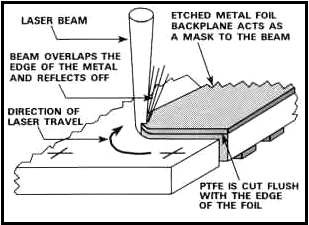
PROGRAMMED SCAN METHOD
Using this method, the etched metal foil on the ground-plane side of the laminate is being used as a mask to create a cut flush with the edge of the foil. The laser beam is traveling along the edge of the metalization on a path defined by the motion control program to overlap the edge of the metal slightly. The part of the beam that hits the metal is reflected and the part that hits the substrate cuts through. The result is a cut that is flush with the metal even if the metal edge varies from the programmed location. If the variation is large it may become necessary to make several parallel passes along the edge of the metal.
CUSTOM SCALING OF THE CIRCUIT
Due to the soft nature of PTFE materials, they are subject to dimensional distortion during fabrication. This typically occurs during metal etching and mechanical processing. When tight tolerances are required, this can cause rejection of the parts. Yields can sometimes be improved by electronically scaling both X and Y cut dimensions during laser processing to compensate for the distortion.
CUTTING ACCURACY
-The laser control system uses high resolution optical registration that permits the precise location of machined features in relation to etched metalization patterns.
-There is no substantial relaxation of laser drilled holes after they have been cut.
-There is no tool wear when laser cutting PTFE substrates. Conventional tool life (drill bits and router bits) can be reduced to minutes when cutting ceramic loaded substrates.
-Due to the small kerf of the laser beam, tighter nesting of parts and features is achievable in order to save expensive substrate real estate and reduce finished part costs.
PROTOTYPE CAPABILITY
The laser is an excellent tool to create prototype circuits and to fine tune them for performance. Setup is quicker and less costly than conventional tooling and changes are much easier to make. Turnaround time for prototype parts can generally be accomplished within a few days.