
-Precision Laser Cut PTFE Substrates for High Frequency Circuits
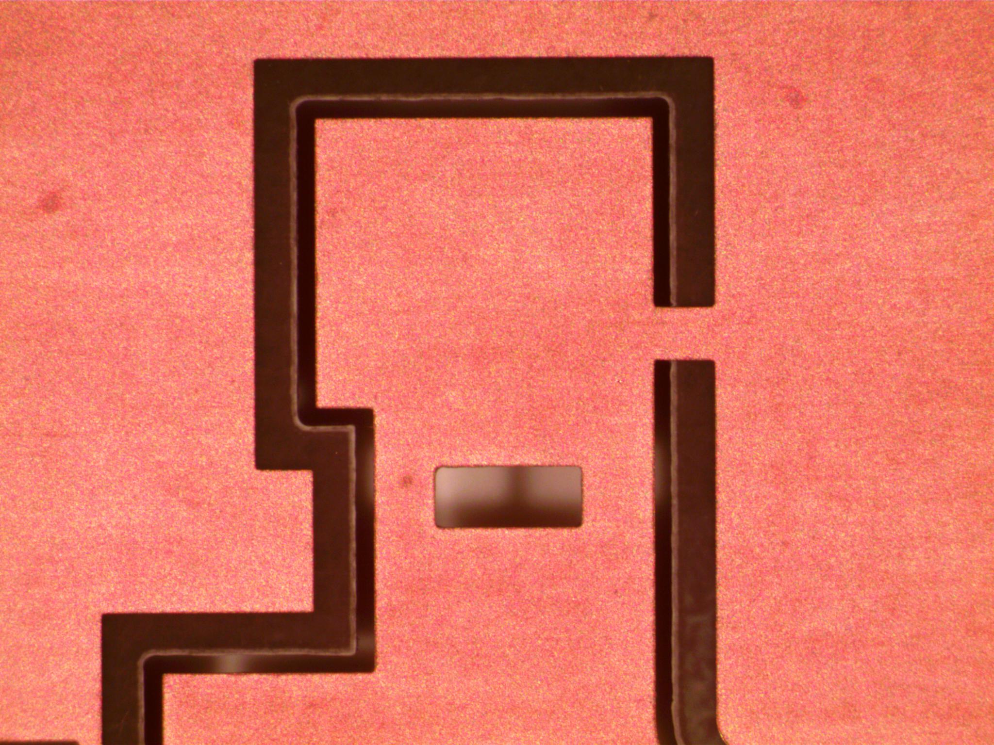
High frequency stripline viewed from the ground plane side
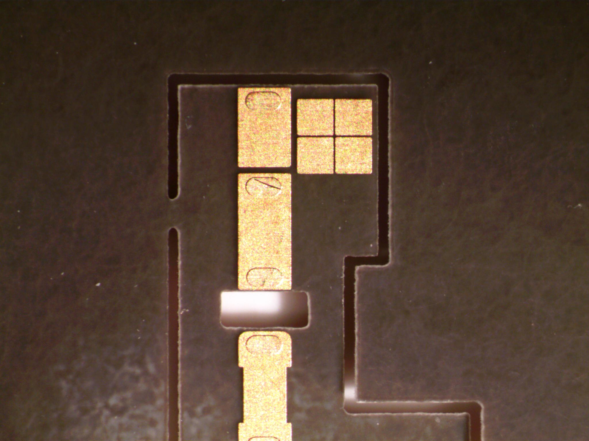
Laser profiled high frequency duroid stripline circuit
APPLICABILITY
This document provides general guidelines and considerations for laser cutting PTFE laminates used in the manufacture of high frequency and microwave circuits. Precision PTFE laminates are used as substrates in the construction of amplifiers, filters, mixers, couplers, phase shifters, transmitters, antennas, etc. PTFE laminate sheet material is sold under the Duroid, Ultralam, Cuclad, Diclad and other trade names.
TYPES OF LAMINATE MATERIALS
The laminates typically used in microstrip, stripline and multilayer circuit fabrication consist of PTFE (Polytetraflouroethylene) that has been reinforced with either glass fibers, woven glass fabric, or proprietary ceramic materials. Certain types of filler materials are used to control the substrate dielectric constant and its temperature coefficient.
PHYSICAL AND MECHANICAL CHARACTERISTICS
Laminates are normally supplied with copper or brass cladding that may be etched and then die cut or precisely machined into the final circuit configuration. The completed laminates are typically between 0.005 and 0.060 inches thick and are clad with 0.125 to 0.5 oz. per ft2 copper. The laminates may then be assembled into an electronic module that serves as a ground plane, a mounting base, and a heat sink. In other cases, the laminates may be bonded to a thick metal plate that serves as the mounting base and the heat sink.
CUTTING LAMINATES REQUIRES PRECISION
Considerable dimensional precision and stability are required of the fabricated circuits to obtain acceptable performance at high frequency. This is particularly true for microstrip and stripline circuits. It is not uncommon to require that line width and spacing dimensions be held to within ± 0.001 inch and that dimensional stability over temperature be less than 25 PPM per C. Workmanship during fabrication must be absolutely meticulous to avoid scratches and micro-dents to edges and surfaces.
The non-rigid nature of unbonded laminates together with the required dimensional tolerances place a substantial demand on the quality and creativity of fixtures, tooling, and workmanship.
CIRCUIT LAYOUTS ARE CHALLENGING
Layout patterns for high frequency circuits are often complex. Additional complexity is created by layout nesting techniques that are employed to fully utilize costly laminate materials. Finally, the fabrication drawings provided may be somewhat inadequate to ensure a precision fit in a housing. Dimensional “fine tuning” may be required to optimize performance of the circuit.
CIRCUIT FABRICATION METHODS USED
Fabrication methods currently used in the industry consist of six basic manufacturing processes:
Masking and etching
Routing with a router
Cutting with a CO2 Laser
Through-hole plating
Drilling with a bit
Punching with a die set
COMPARISON OF CIRCUIT FABRICATION METHODS
Precision photo masking and etching are generally adequate to produce metal patterns of the desired accuracy on the substrate. The table below attempts to qualitatively show three common methods used to shape a laminate substrate. The “best” method will depend on the laminate materials, the geometry of the specific circuit configuration, the tooling available, and, as in most precision operations, the skills, tools, and ingenuity of the operator. The selection of a skilled, experienced, and committed supplier is the best recommendation for achieving a high quality, cost effective product.
DESIRABLE ATTRIBUTE OR CIRCUIT APPLICATION PRECISION ROUTER AND DRILL CO2 LASER CUT PUNCH AND DIE
ACCURACY OF FABRICATION MED HIGH LOW
TOOLING TURNAROUND TIME N/A N/A LONG
ABILITY TO MAKE CHANGES FAST FAST SLOW
LOW VOLUME APPLICATIONS GOOD GOOD POOR
HIGH VOLUME APPLICATIONS FAIR GOOD GOOD
SUBSTRATE WITH CERAMIC FILL POOR GOOD FAIR
SUBSTRATE WITH GROUND PLANE FAIR GOOD NO
ABILITY TO CUT THROUGH COPPER YES POOR YES
PROGRAMMED PATH DESIGN YES YES YES
PROGRAMMED SCAN DESIGN NO YES NO
SCALING TO MATCH PATTERN DIFFICULT YES NO
SHARP CORNERS/CLEAN EDGES POOR GOOD FAIR
OVERALL PART QUALITY MED HIGH MED
HOW THE LASER CUTS PTFE LAMINATES
The laser cutting process uses infrared light focused to a small spot (approx. 0.005 in.) to cut through the substrate material. PTFE, glass, and filler materials readily absorb this laser energy and are easily cut. The metallization is very reflective to the laser beam so it resists cutting. This selective nature of the CO2 energy absorption enables it to cut along the edge of metallization without damaging it. In some cases it is possible to remove the substrate material down to a metal layer to form blind vias and cavities.
LASER FLEXIBILITY
-The laser is a single tool that can perform most of the required material removal processes without the need for additional handling and multiple tool changes.
-The laser is effective for “Programmed Path”, “Programmed Scan” and “Raster Scan” methods of cutting and material removal. This flexibility permits optimization of the layout based on the types of features being created and the requirement to save costly laminate real estate.
-Holes can be virtually any size or shape due to the small beam size and programmable motion.
-Beam focus provides a modest degree of control over the shape of the substrate edge.
-Either backside or frontside processing can be performed by the laser.
LASER CUT QUALITY
Compared to other cutting/punching methods, the laser cut is quite precise and does not distort adjacent material.
-The laser cut leaves an extremely clean, sharp edge and produces square corners.
-Laser cutting of tight, intricate patterns is generally fast and accurate.
PROGRAMMED PATH METHOD
The shape of the cut is determined entirely by the programmed path in the motion control system. This technique usually utilizes the laser optical registration system to precisely locate and control the cut with respect to alignment targets or to a specific feature on the laminate such as the edge of the etched metal foil. In this case, a set-back is required from the edge of the laminate to the edge of the etched foil. If the cut must be right up to the edge of the metallization, the programmed scan method can be used (see below).
PROGRAMMED SCAN METHOD
Using this method, the etched metal foil on the ground-plane side of the laminate is being used as a mask to create a cut flush with the edge of the foil. The laser beam is travelling along the edge of the metallization on a path defined by the motion control program to overlap the edge of the metal slightly. The part of the beam that hits the metal is reflected and the part that hits the substrate cuts through. The result is a cut that is flush with the metal even if the metal edge varies from the programmed location. If the variation is large it may become necessary to make several parallel passes along the edge of the metal.
CUSTOM SCALING OF THE CIRCUIT
Due to the soft nature of PTFE materials, they are subject to dimensional distortion during fabrication. This typically occurs during metal etching and mechanical processing. When tight tolerances are required, this can cause rejection of the parts. Yields can sometimes be improved by electronically scaling both X and Y cut dimensions during laser processing to compensate for the distortion.
CUTTING ACCURACY
-The laser control system uses high resolution optical registration that permits the precise location of machined features in relation to etched metallization patterns.
-There is no substantial relaxation of laser drilled holes after they have been cut.
-There is no tool wear when laser cutting PTFE substrates. Conventional tool life (drill bits and router bits) can be reduced to minutes when cutting ceramic loaded substrates.
-Due to the small kerf of the laser beam, tighter nesting of parts and features is achievable in order to save expensive substrate real estate and reduce finished part costs.
PROTOTYPE CAPABILITY
The laser is an excellent tool to create prototype circuits and to fine tune them for performance. Setup is quicker and less costly than conventional tooling and changes are much easier to make. Turnaround time for prototype parts can generally be accomplished within a few days.