Precision Laser Cutting of PTFE Substrates (Duroid) for High Frequency Circuits
APPLICABILITY
This document provides general guidelines and considerations for laser cutting PTFE laminates used in the manufacture of high frequency and microwave circuits. Precision PTFE laminates are used as substrates in the construction of amplifiers, filters, mixers, couplers, phase shifters, transmitters, antennas, etc. PTFE laminate sheet material is sold under the Duroid, Ultralam, Cuclad, Diclad and other trade names.
TYPES OF LAMINATE MATERIALS
The laminates typically used in microstrip, stripline and multilayer circuit fabrication consist of PTFE (Polytetraflouroethylene) that has been reinforced with either glass fibers, woven glass fabric, or proprietary ceramic materials. Certain types of filler materials are used to control the substrate dielectric constant and its temperature coefficient.
PHYSICAL AND MECHANICAL CHARACTERISTICS
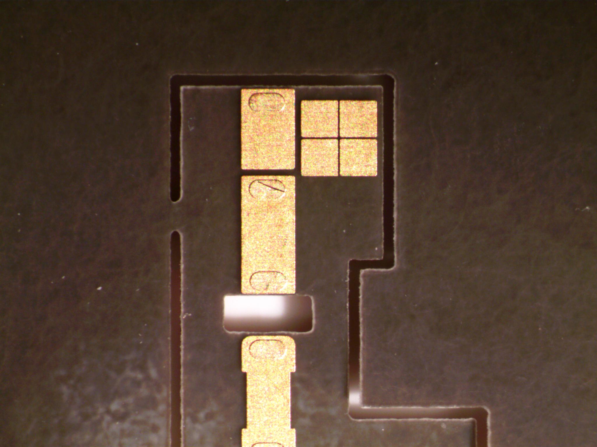
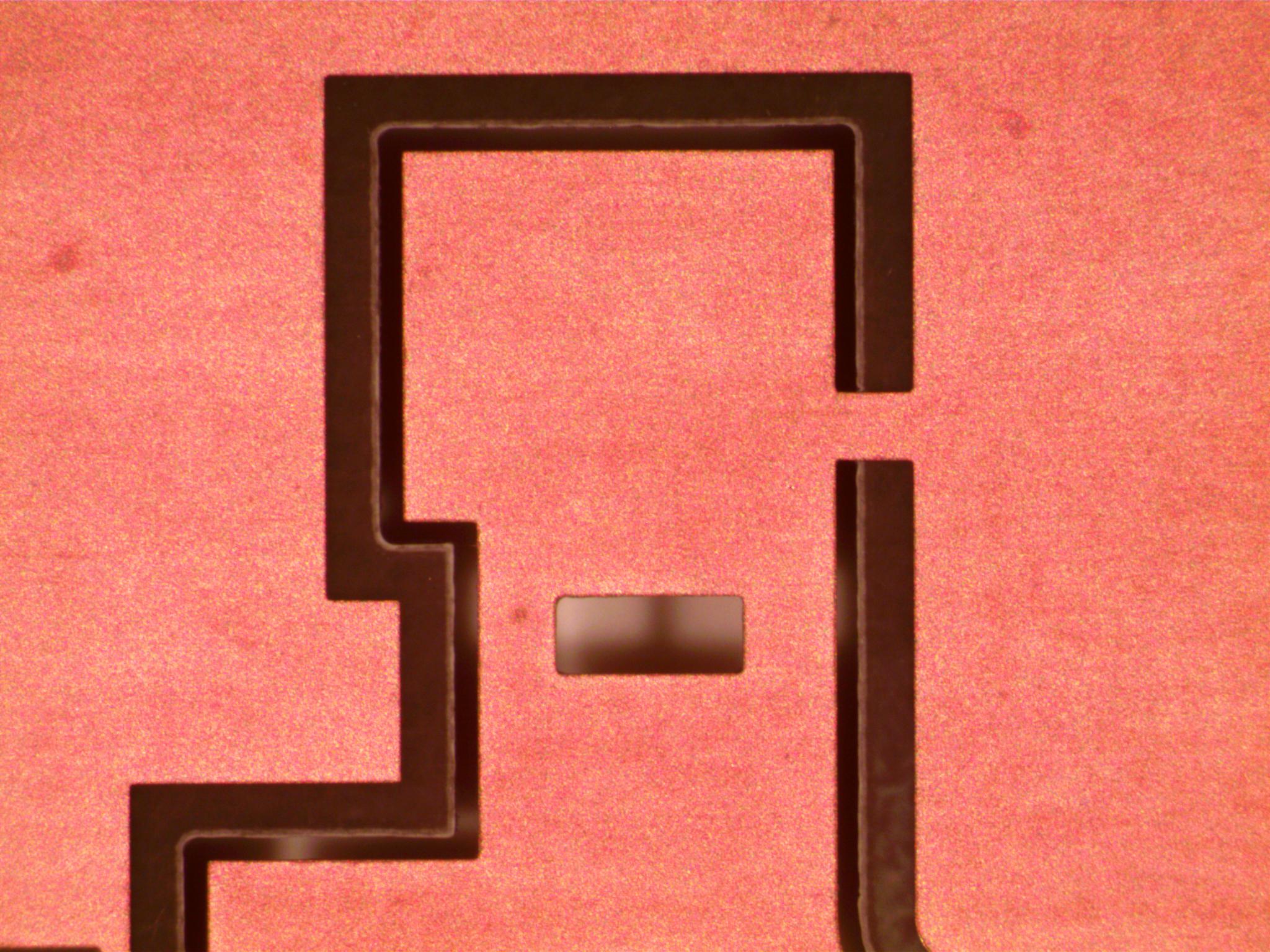
Laminates are normally supplied with copper or brass cladding that may be etched and then die cut or precisely machined into the final circuit configuration. The completed laminates are typically between 0.005 and 0.060 inches thick and are clad with 0.125 to 0.5 oz. per ft2 copper. The laminates may then be assembled into an electronic module that serves as a ground plane, a mounting base, and a heat sink. In other cases, the laminates may be bonded to a thick metal plate that serves as the mounting base and the heat sink.
CUTTING LAMINATES REQUIRES PRECISION
Considerable dimensional precision and stability are required of the fabricated circuits to obtain acceptable performance at high frequency. This is particularly true for microstrip and stripline circuits. It is not uncommon to require that line width and spacing dimensions be held to within ± 0.001 inch and that dimensional stability over temperature be less than 25 PPM per C. Workmanship during fabrication must be absolutely meticulous to avoid scratches and micro-dents to edges and surfaces.
The non-rigid nature of unbonded laminates together with the required dimensional tolerances place a substantial demand on the quality and creativity of fixtures, tooling, and workmanship.
CIRCUIT LAYOUTS ARE CHALLENGING
Layout patterns for high frequency circuits are often complex. Additional complexity is created by layout nesting techniques that are employed to fully utilize costly laminate materials. Finally, the fabrication drawings provided may be somewhat inadequate to ensure a precision fit in a housing. Dimensional “fine tuning” may be required to optimize performance of the circuit.
CIRCUIT FABRICATION METHODS USED
Fabrication methods currently used in the industry consist of six basic manufacturing processes:
Masking and etching
Routing with a router
Cutting with a CO2 Laser
Through-hole plating
Drilling with a bit
Punching with a die set
COMPARISON OF CIRCUIT FABRICATION METHODS
Precision photo masking and etching are generally adequate to produce metal patterns of the desired accuracy on the substrate. The table below attempts to qualitatively show three common methods used to shape a laminate substrate. The “best” method will depend on the laminate materials, the geometry of the specific circuit configuration, the tooling available, and, as in most precision operations, the skills, tools, and ingenuity of the operator. The selection of a skilled, experienced, and committed supplier is the best recommendation for achieving a high quality, cost effective product.