
UV Laser Processing
For precision jobs and intricate layers, Ultraviolet (UV) laser technology is useful for its shorter wavelengths. The higher energy produced makes it suitable to mark and machine complex materials in small, focused spots, careful not to damage deeper layers.
UV lasers are ideal for processing thin metals like copper sheet, brass, stainless steel, silver, and aluminum. Other materials include thin epoxy blends, plastics, polycarbonates, Kapton, ALN, ferrite, Kovar, gold, mylar, nickel, and more.
Marking by UV laser is far more practical today. They finish cleaner than traditional tools or ink used to mark or machine. In the medical industry, UV allows for minimal contamination. UV lasers lessen the heat stress caused by other systems, therefore leaving less soot and/or burrs.
Aerospace, automotive, defense, and electronics industries heavily rely on UV laser marking capabilities for authenticating parts.
More About UV Laser Capabilities
Micro Via Drilling
Micro Vias are generally described as a via or hole through one or more layers of a flexible circuit board made of laminations of alternating insulating and conducting layers of material. These layers are usually made of copper sheet and thin epoxy-fiberglass blend. The laser drilling tool will create a via from the top layer down to a copper catch pad below. This via will be plated to form an electrical connection between conducting layers.
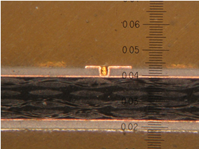
Figure 1: First layer, Copper plated micro via in a Printed Circuit Board
The drilling and subsequent plating works best when the diameter of the via is equal to or greater than the depth of the via (a 1:1 ratio is ideal). Accu-Tech regularly generates vias in the range of .003” to .008” (.075 -.100mm). There is the capability to produce smaller and larger sizes.
For helpful links to information on the PCB industry, check the IPC website
Flex Circuits
UV laser technology is an excellent tool for precision singulation of circuits generated in an array on flex panels. The laser’s very small ‘tool size’, as well as no contact forces, may be very beneficial on small parts or parts with chip components already attached.
Our lasers generate very little smoke or carbon deposits on the edges of the parts therefore reducing cleaning time. Our fixturing prevents parts from dropping or displacing after the final cut, reducing risk to fragile parts.
For an additional cost, we can accommodate flexible circuits with stiffeners and/or components applied. In most cases, we can hold flex circuit accuracy to +/-.001″.
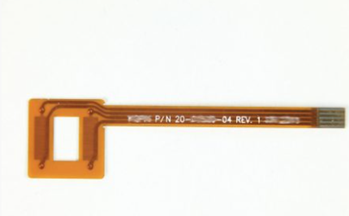
Figure 2: Flex Circuit
Board Rework and Recovery Solutions
Whether errors occur in design or production, you may be able to salvage your product. Methods include selective solder mask removal, controlled depth coverlay/dielectric removal, squeeze out removal, pad isolation, and precision trace trimming.
Skiving/ Ablation
Skiving allows for the controlled removal of material. Typical applications are flying leads, pad exposures for flex circuits, or cavity formation on rigid circuits. Laser skiving can be performed to remove dielectric material or to stop without cutting all the way through (controlled depth).
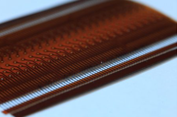
Figure 3: Ablation of flying leads
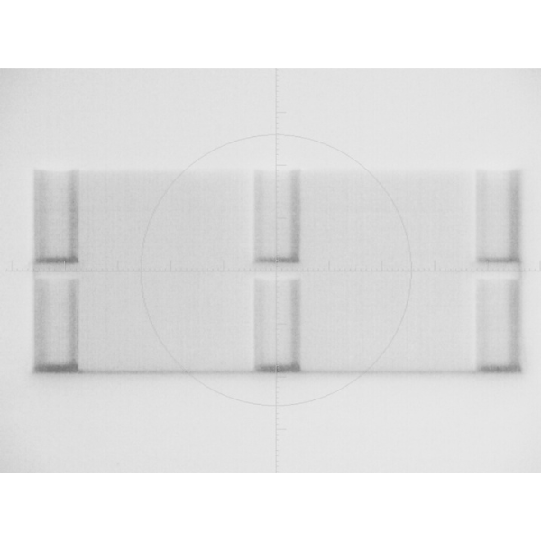
Figure 4: Cavity Ablation
Targeting and Aligning
Accu-Tech can align to pre-etched openings in the top layer and remove the dielectric down to the next layer. Likewise, we can create openings in a solid copper top layer aligned to your lower layer registration fiducials and then remove the dielectric. Supplying pre-etched openings in the top layer may be more cost effective – depending on your etching capabilities. Pre-etched boards can have a quicker turnaround time as well.
Registration targeting is usually a set of four butterfly, crosshair, and bullseye targets, one at each corner of the panel just outside of the pattern of the part or parts. As well, this allows our systems to compensate for the slight shrinkage and out-of-square conditions that can be an outcome of the lamination process.
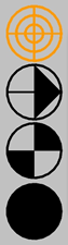
Figure 5: Fiducials
We can accommodate prototyping high-volume production quantities.
Any overhanging or excess copper flashing from lamination should be pre-trimmed from the boards before delivery as this excess material can prevent the boards from lying flat on the laser tooling.
Guidelines for VIA drill files:
- We can accept .DRL files (ideal), Gerber or .DXF files.
- Files must have different via sizes called out as different tool numbers all in the same file.
- One file per side/layer.
- Fiducials should be identified as a separate tool number as well. We prefer these targets to be under .020” in diameter and can be of the butterfly, bullseye, circular pad, or crosshair type.
- It is helpful to include tooling holes or landmarks to help quickly identify panel orientation.
- Please send a panel stack-up showing the thickness of materials we are drilling through and landing on. This will help us in reducing the time for test patterns which reduces costs to you.